
Frequently Asked Questions
Common-mode voltage (\(V_{cm}\)) represents the average voltage of two signal lines with respect to a common reference point, typically ground. It is essential in differential signal systems, power electronics, and EMC testing.
The common-mode voltage is mathematically defined as:
\(V_{cm} = \frac{V_+ + V_-}{2}\)
Where:
– \(V_+\) is the voltage on the positive signal line relative to ground
– \(V_-\) is the voltage on the negative signal line relative to ground
To measure Vcm:
- Oscilloscope: Connect probes to \(V_+\) and \(V_-\), measure each with respect to ground, and compute the average.
- Differential Probe: Use to extract both differential and common-mode signals.
- Multimeter: For DC or low-frequency, measure \(V_+\) and \(V_-\) relative to ground and average them.
Measuring Vcm helps identify noise, verify balance, and improve performance.
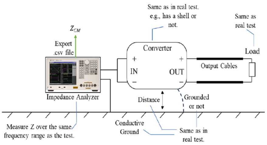
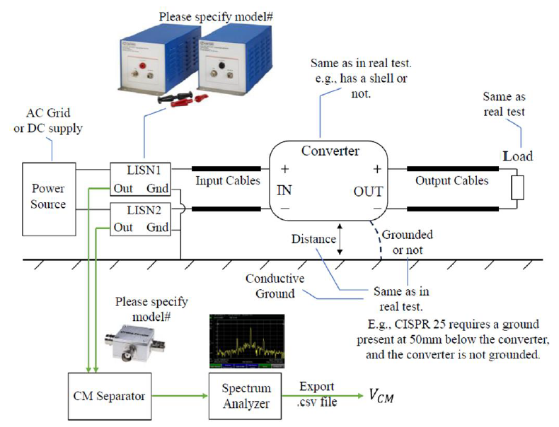
Common-mode impedance (\(Z_{cm}\)) is the impedance that common-mode currents encounter between signal lines and ground.
To measure \(Z_{cm}\) accurately, use an impedance analyzer (e.g., Keysight E4990A). Connect the two signal lines together to form a common-mode path, then measure the impedance between this node and ground.
Alternatively, use a Vector Network Analyzer (VNA) with a mode-conversion setup to measure \(Z_{cm}\) using mixed-mode S-parameters.
For a basic estimation, inject a common-mode signal into the system and measure voltage and current. Then calculate:
\(Z_{cm} = \frac{V_{cm}}{I_{cm}}\)
Proper grounding and shielding are essential to reduce noise and ensure accurate readings.
Insertion Loss (IL) is a fundamental parameter used to describe how much signal power is lost when a component, such as a filter, connector, or cable, is inserted into a transmission path. It is typically expressed in decibels (dB) and is crucial in high-frequency, RF, and communication systems, where maintaining signal strength and quality is important.
The insertion loss quantifies the difference in signal amplitude or power before and after the device under test (DUT). The voltage-based formula for insertion loss is:
\(\text{Insertion Loss (dB)} = 20 \log_{10} \left( \frac{V_{\text{in}}}{V_{\text{out}}} \right)\)
Where:
\(V_{\text{in}}\) is the voltage before the DUT
\(V_{\text{out}}\) is the voltage after the DUT
For power-based measurements, the equation becomes:
\(\text{Insertion Loss (dB)} = 10 \log_{10} \left( \frac{P_{\text{in}}}{P_{\text{out}}} \right)\)
A higher insertion loss indicates greater signal attenuation. For example, an insertion loss of 3 dB means approximately 50% of the power is lost. Insertion loss is often measured using a Vector Network Analyzer (VNA), which directly measures transmission parameters such as S21.
A Large Language Model (LLM) is a type of artificial intelligence designed to understand and generate human language. LLMs are built using deep learning techniques, especially the transformer architecture, which enables them to analyze context and generate coherent text.
Below is a simplified diagram showing the core of an LLM — the Transformer Block:
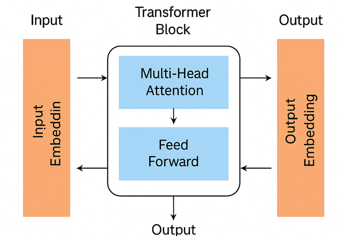
Diagram: The transformer architecture behind large language models.
🔹 1. Input Embedding
Text is first converted into a format the model can understand — numerical vectors — using a process called embedding. These vectors represent the meaning and position of each word.
🔹 2. Multi-Head Attention
This is how the model determines which words in the input are most relevant to each other. It can focus on multiple relationships at once, which helps it understand context.
🔹 3. Feed Forward Network
After attention is applied, the data is processed through a small neural network to refine the result.
🔹 4. Output Embedding
The final output is converted into predictions — such as the next word in a sentence — or passed on to deeper layers for further processing.
LLMs like ChatGPT use stacks of these transformer blocks to power natural conversations, summarize information, write code, and more — all by predicting the most likely next token in a sequence.
Leakage current refers to the current that flows from live conductors to the ground line through insulation materials or capacitors under normal operating conditions. In electronic devices, this current primarily flows through Y capacitors (safety capacitors) from the live or neutral line to the protective ground line. The leakage current is directly proportional to the Y capacitor value, following the formula:
Leakage Current = Grid Voltage × 2π × Frequency × Y Capacitor Value
Practical Examples (230V/50Hz grid):
- Y capacitor = 2.2nF → Leakage current ≈ 0.16mA
- Y capacitor = 4.7nF → Leakage current ≈ 0.34mA
- Y capacitor = 10nF → Leakage current ≈ 0.72mA
- Y capacitor = 22nF → Leakage current ≈ 1.59mA
As demonstrated, when the Y capacitor value doubles, the leakage current also doubles proportionally.
Risks of Increasing Y Capacitor Values
While increasing Y capacitor values can improve EMI performance, it introduces several concerns:
- Increased Safety Risk: Higher leakage current may exceed safety standard limits
- Increased Power Consumption: Device standby power consumption rises
- Certification Difficulties: May fail to pass safety certifications in various countries
Safety Standard Considerations
Different application scenarios require compliance with different safety standards, each with varying leakage current requirements, thus affecting Y capacitor selection:
- Household Appliances (IEC 60335): Typically require AC leakage current peak ≤ 0.7mA
- IT Equipment (IEC 60950-1/IEC 62368-1): Usually require fixed equipment leakage current ≤ 3.5mA
- Industrial Equipment: Requirements are relatively relaxed, with specific values varying by standard
Design Recommendations
In summary, Y capacitor value selection requires finding the optimal balance between EMI performance and leakage current safety. In electronic device design, consider the following aspects:
- Identify applicable safety standards and leakage current limits for your product
- Calculate the maximum allowable Y capacitor value based on actual grid parameters
- Validate design effectiveness through testing
- Consider the most stringent requirements for global products
The key principle is that safety must always come first – while EMI performance can be improved through other methods, exceeding leakage current limits poses potential safety hazards.
Imagine you’ve designed an excellent switching power supply – highly efficient, low cost, and outstanding performance. However, when it operates:
– The nearby radio produces static noise
– WiFi signals deteriorate
– Other electronic devices malfunction
– It may even affect the normal operation of medical equipment
This is the real-world impact of EMI (Electromagnetic Interference), which refers to the adverse effects caused by electromagnetic energy generated by electronic devices during operation on other equipment.
EMI can be understood as “noise pollution” in the electromagnetic environment. The switching power supply acts as a noise source, where switching actions generate high-frequency electromagnetic energy, just as naturally as a car engine produces mechanical noise. When these “electromagnetic noises” become strong enough, they will interfere with the normal operation of surrounding electrically-powered devices.
Just as automotive noise is regulated by relevant laws and regulations, the electromagnetic noise (EMI) generated by electronic devices must also comply with relevant regulatory standards before they can enter the market.
EMI filter design primarily refers to the reasonable combination of chokes and X/Y capacitors that compose the filter. Based on this foundation, consideration is then given to the proper layout of components within the filter, as well as the layout relationships with other converter components, to minimize the adverse effects of parasitic parameters on filter performance as much as possible.
Key Considerations for Selecting Filter Components
1. Rated Voltage and Current: Must meet your application requirements. Voltage or current exceeding the filter’s rated values will damage the filter.
2. Impedance vs. Frequency Characteristics: Choke datasheets typically provide curves showing how choke impedance varies with frequency, usually expressed in Ω. Higher impedance means stronger blocking capability for noise in corresponding frequency ranges. However, although most datasheets only provide magnitude curves for choke impedance, focusing solely on impedance magnitude is one-sided. The phase of impedance is equally important, as this is closely related to potential resonance.
3. Insertion Loss: Choke datasheets sometimes provide insertion loss test data for reference, which indicates the strength of filtering capability. Larger values mean better filtering effects, typically expressed in dB. However, insertion loss measurements are usually based on 50-ohm source and load impedance assumptions, which typically do not match actual conditions. Therefore, the actual noise attenuation by chokes often differs significantly from datasheet insertion loss values. Accurate results require calculations based on the converter’s actual conditions.
Common EMI Filter Application Misconceptions
Misconception 1: Bigger filters are always better
Oversized filters waste cost and space, and may introduce new resonance problems. Selection should be based on actual needs.
Misconception 2: One filter solves all problems
Sometimes multi-stage filtering is needed. Different types of noise require different filtering methods. Systematic consideration is more important.
Misconception 3: Only considering filters at the end
It’s best to consider filters from the initial design stage. Source control is more effective than end-stage filtering. Filters are only one part of EMI control.
There are numerous factors affecting the EMI of a power electronic converter. Diagnosing the causes of EMI generation in a power electronic converter requires professional EMI knowledge. The following lists common factors that can influence the EMI generated by converters.
1. Switching Characteristics
- Switching Frequency – Higher frequency generates richer high-frequency harmonics, making EMI problems more severe.
- Switching Speed (dv/dt and di/dt) – Faster switching devices create greater voltage and current change rates, generating stronger EMI energy.
- Switching Waveform Quality – Ideal square-wave switching generates less EMI than waveforms with ringing and overshoot.
- Dead Time – Improper dead time settings lead to non-ideal switching processes, increasing EMI.
2. Circuit Topology
- Topology Type – Hard-switching topologies generate more EMI than soft-switching topologies; isolated topologies have more complex EMI propagation paths than non-isolated ones.
- Number of Switching Devices – More devices increase the probability of simultaneous switching, making EMI superposition effects more prominent.
- Current Path – Longer high-frequency current paths and larger loop areas result in stronger radiated EMI.
- Grounding Method – Improper grounding increases common-mode EMI; multi-point grounding may form ground loops.
3. Component Parameters
- Power Device Characteristics – Different switching characteristics of MOSFETs, IGBTs, and other devices directly affect EMI levels.
- Parasitic Parameters – Parasitic inductance and capacitance of devices and PCB cause oscillations, increasing EMI.
- Driver Circuit – Drive strength affects switching speed; driver circuit design influences switching waveform quality.
- Diode Reverse Recovery – Poor reverse recovery characteristics of freewheeling diodes generate severe high-frequency oscillations.
4. Circuit Parameters
- Power Level – Higher power means greater switching currents, generating stronger EMI energy.
- Input/Output Voltage – Higher voltages result in greater dv/dt during switching, making EMI more severe.
- Load Characteristics – Load impedance characteristics affect current waveforms, which in turn affect EMI.
- Resonant Frequency – If LC resonant frequencies in the circuit fall within sensitive frequency bands, they amplify EMI in those bands.
5. Physical Structure and Layout
- PCB Layout – Trace length, width, number of layers, and via design all affect parasitic parameters and EMI propagation.
- Component Placement – Distance and orientation of high-frequency components affect mutual coupling and radiated EMI.
- Heat Sink Design – Metal heat sinks may act as antennas, amplifying radiated EMI.
- Mechanical Structure – Enclosure shielding effectiveness and opening sizes affect EMI leakage.
6. Control Strategy
- Modulation Method – Different modulation methods like PWM and PFM have different spectral distributions and distinct EMI characteristics.
- Frequency Dithering Technology – Spread spectrum modulation can disperse EMI energy, reducing peak values.
- Synchronous Control – Phase relationships in multi-phase converters affect EMI mutual cancellation effects.
- Soft Switching Control – Soft switching technologies like ZVS and ZCS can significantly reduce EMI.
7. External Environmental Factors
- Power Quality – Harmonics and noise in the input power supply are amplified and propagated through the converter.
- Load Changes – Sudden load changes cause current impacts, generating transient EMI.
- Temperature Effects – Temperature changes affect device parameters, which in turn affect switching characteristics and EMI.
- Surrounding Electromagnetic Environment – External electromagnetic fields may affect converter EMI performance through coupling.
8. Filtering and Protection Measures
- Input Filter – Improper filter parameter design may cause resonant amplification at certain frequencies.
- Output Filtering – Insufficient output filtering allows high-frequency components to propagate to the load side.
- Shielding Effectiveness – Incomplete electromagnetic shielding increases radiated EMI leakage.
- Grounding System – Grounding impedance and ground loops affect EMI propagation paths.
Basic Concept Understanding
- Differential Mode Noise (DM)
- Noise current forms a loop between two conductors, such as live and neutral wires, or positive and negative power supply conductors.
- Just like normal load current, but with very high frequency.
- Common Mode Noise (CM)
- Noise current flows between conductors and ground, for example, flowing out of the converter through both live and neutral wires (currents in the same direction), then returning through ground or other paths.
- This is an “unexpected” current path.
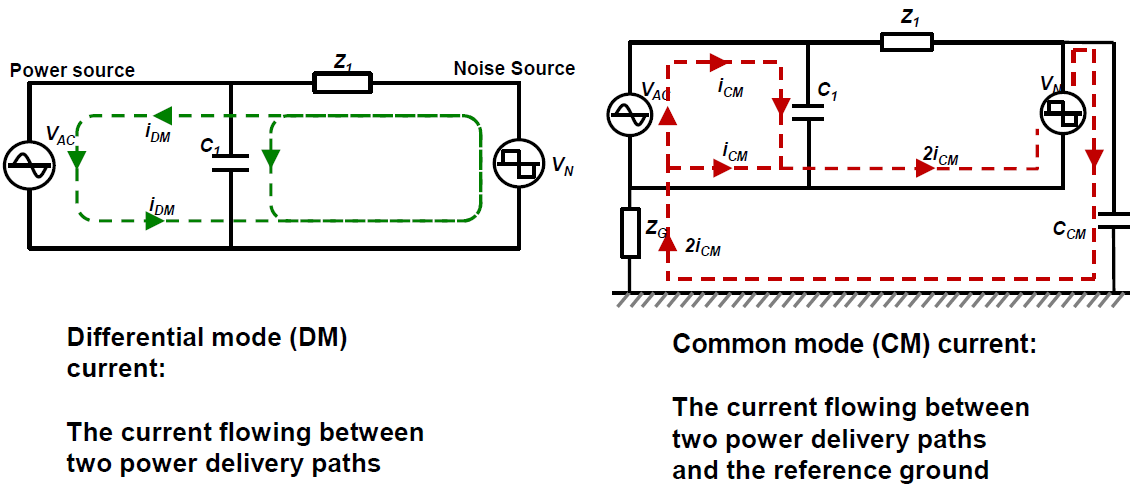
Visual Understanding
Imagine a dual-lane highway:
- Differential Mode Noise = Vehicles traveling in opposite directions on two lanes
- Noise “flows” between two power lines in opposite directions
- Current goes out and returns, forming a complete loop
- Just like normal power transmission, but at high frequency
- Common Mode Noise = Vehicles traveling in the same direction on both lanes
- Noise “flows in the same direction” on both wires
- Must return through ground wire or other paths
- This is an abnormal transmission mode
Simple Understanding: EMI Testing is Like a “Medical Checkup”
Imagine that your designed power electronic converter is like a person, and EMI testing is giving it a “comprehensive medical checkup” to examine whether it will “infect” other devices, or whether it will be “infected” by other devices.
Purpose of EMI Testing
Verify if your product “follows the rules”:
- Measure how strong the electromagnetic noise generated by the product is
- Verify whether it exceeds regulatory limits
- Ensure the product will not interfere with other devices
Just as cars must pass exhaust emission tests before they can be driven on roads, electronic products must pass EMI testing before they can be sold.
How is the Testing Actually Done?
Conducted Emission Testing:
- Connect your product to specialized test equipment (LISN)
- LISN is like an “electromagnetic stethoscope” that can “hear” high-frequency noise on power lines
- Test instruments will tell you how strong the noise is and its frequency distribution
- As simple and intuitive as measuring blood pressure
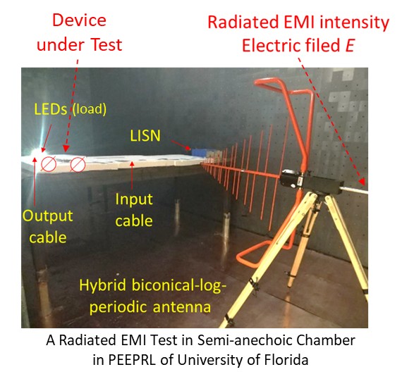
Radiated Emission Testing:
- Place the product in a specialized test room (anechoic chamber)
- Room walls are covered with wave-absorbing materials, like soundproofing in a recording studio
- Use antennas to “listen” to electromagnetic waves radiated outward by the product
- Measure radiation intensity in different directions and at different frequencies
What Do Test Results Tell You?
Spectrum Plot:
- Horizontal axis is frequency, vertical axis is interference intensity
- Like an ECG, it can show where the problems are
- Areas exceeding the red line (limit values) are where improvements are needed
Specific Data:
- Which frequency points exceeded limits
- How many dB over the limit
- Whether it’s a conduction problem or radiation problem
- Whether it’s differential mode interference or common mode interference
Why Conduct EMI Testing?
Regulatory Requirements:
- Almost all countries require EMC certification
- Products cannot be sold without test reports
- This is the product’s “birth certificate”
Technical Needs:
- Help you discover problems in the design
- Ensure product quality and reliability
- Guide you on how to improve the product, just like discovering problems in a medical checkup:
- Find the “cause”: Is it a switching frequency problem? Layout problem? Or insufficient filtering?
- “Prescribe treatment”: Adjust parameters, improve design, add filtering
- “Follow-up examination”: Re-test to verify improvement effects
Commercial Value:
- Products that pass testing are more easily accepted by customers
- Avoid after-sales problems and complaints
- Enhance brand image and competitiveness
Testing Costs and Timeline
Cost Considerations:
- Formal testing costs typically range from tens of thousands to hundreds of thousands
- Pre-testing costs are relatively inexpensive
- Passing once is more economical than repeated testing
Time Planning:
- Formal testing usually takes 1-2 weeks
- If it fails, you need to reschedule
- Recommend doing pre-testing first, then formal testing after confirming no issues
Practical Recommendations
Consider During Design Phase:
- Don’t wait until the product is finished to think about EMI
- Early prevention costs much less than later treatment
Choose the Right Testing Institution:
- Select qualified certification laboratories
- Preferably choose experienced institutions
- They can provide professional remediation suggestions
Prepare Well for Testing:
- Prepare complete technical documentation
- Ensure prototype status is stable
- Reserve sufficient time and budget
EMI testing is not a burden, but a tool to help you design better products. Just as medical checkups help you maintain health, EMI testing helps your products maintain “electromagnetic health”!
Simple Understanding: “Unexpected Guests” in Circuits
Imagine you designed an ideal circuit with only the resistors, inductors, and capacitors you need. But after actual manufacturing, some components appear in the circuit that you did not design but actually exist — these are parasitic parameters.
Why Do Parasitic Parameters Occur?
Reality of the Physical World:
- Any conductor has resistance (even if very small)
- Any current-carrying conductor has a magnetic field around it (producing inductance)
- Any two nearby conductors have an electric field between them (producing capacitance)
These are physical laws that cannot be completely avoided.
For Example: A simple wire is ideally just a wire, but in reality:
- The wire itself has resistance (parasitic resistance)
- The wire has a magnetic field around it (parasitic inductance)
- The wire has an electric field between it and ground or other wires (parasitic capacitance)
Main Parasitic Parameters in Power Electronic Circuits
1. Parasitic Inductance
- Sources: PCB traces, component leads, connecting wires
- Characteristics: Impedes current changes, has significant impact at high frequencies
- Manifestation: Generates voltage spikes and oscillations during switching
- Real-world Impact Example:
- When your switching device turns off, parasitic inductance generates reverse voltage spikes
- Like suddenly closing a water tap causing water hammer phenomenon
2. Parasitic Capacitance
- Sources: Between PCB layers, between components, between heat sinks and circuits
- Characteristics: Becomes low-impedance path at high frequencies
- Manifestation: High-frequency noise easily couples and propagates
- Real-world Impact Example:
- Parasitic capacitance between switching devices and heat sinks transfers noise to the heat sink
- Heat sink becomes an “antenna” radiating EMI outward
3. Parasitic Resistance
- Sources: Wire resistance, via resistance, solder joint resistance
- Characteristics: Consumes power, creates voltage drops
- Manifestation: Reduced efficiency, increased heat generation
Impact of Parasitic Parameters on EMI
Generating Oscillations:
- Parasitic inductance and capacitance form LC oscillating circuits
- Switching actions excite oscillations, generating high-frequency noise
- Like striking a tuning fork to produce resonance
Changing Current Paths:
- At high frequencies, parasitic capacitance becomes low impedance
- Current will “choose” unexpected paths to flow
- Original filter designs may become ineffective
Amplifying Interference:
- Parasitic parameters may produce resonance at certain frequencies
- Interference at those frequencies gets amplified
- EMI exceeds limits at specific frequency points
Simple Understanding: EMI Filters as “Silencers” for Electromagnetic Noise
Imagine a car’s muffler that reduces engine noise without affecting the surrounding environment. An EMI filter is like a “silencer” in electrical circuits, specifically designed to reduce electromagnetic noise generated by power electronic converters.
Functions of EMI Filters (Bidirectional Protection)
External Protection: Prevents your device from interfering with other devices
Internal Protection: Prevents external interference from affecting your device’s operation
Working Principle of EMI Filters (Frequency Selectivity)
Allows low-frequency power signals to pass through smoothly (DC voltage and current from power supplies, or 50Hz/60Hz AC voltage and current)
Absorbs or reflects high-frequency noise generated by switching (from tens of kHz to tens of MHz)
Core Components of EMI Filters
Inductors (Chokes):
- Function: Block high-frequency currents from passing through
- Characteristics: Higher frequency results in greater impedance
Capacitors (X/Y capacitors):
- Function: Provide bypass paths for high-frequency noise
- Characteristics: Higher frequency results in lower impedance
Resistors (Sometimes):
- Function: Consume noise energy and prevent resonance
EMI filter design primarily refers to the reasonable combination of chokes and X/Y capacitors that compose the filter. Based on this foundation, consideration is then given to the proper layout of components within the filter, as well as the layout relationships with other converter components, to minimize the adverse effects of parasitic parameters on filter performance as much as possible.
Key Considerations for Selecting Filter Components
1. Rated Voltage and Current: Must meet your application requirements. Voltage or current exceeding the filter’s rated values will damage the filter.
2. Impedance vs. Frequency Characteristics: Choke datasheets typically provide curves showing how choke impedance varies with frequency, usually expressed in Ω. Higher impedance means stronger blocking capability for noise in corresponding frequency ranges. However, although most datasheets only provide magnitude curves for choke impedance, focusing solely on impedance magnitude is one-sided. The phase of impedance is equally important, as this is closely related to potential resonance.
3. Insertion Loss: Choke datasheets sometimes provide insertion loss test data for reference, which indicates the strength of filtering capability. Larger values mean better filtering effects, typically expressed in dB. However, insertion loss measurements are usually based on 50-ohm source and load impedance assumptions, which typically do not match actual conditions. Therefore, the actual noise attenuation by chokes often differs significantly from datasheet insertion loss values. Accurate results require calculations based on the converter’s actual conditions.
Common EMI Filter Application Misconceptions
Misconception 1: Bigger filters are always better
Oversized filters waste cost and space, and may introduce new resonance problems. Selection should be based on actual needs.
Misconception 2: One filter solves all problems
Sometimes multi-stage filtering is needed. Different types of noise require different filtering methods. Systematic consideration is more important.
Misconception 3: Only considering filters at the end
It’s best to consider filters from the initial design stage. Source control is more effective than end-stage filtering. Filters are only one part of EMI control.
X Capacitors
X capacitors are connected between the two power lines (line to neutral, or positive to negative). Their function is to provide a “shortcut” for high-frequency noise, allowing noise to circulate between the two power lines rather than escaping to interfere with other devices.
Y Capacitors
Y capacitors are connected between power lines and the device chassis (ground). Their function is to “drain” high-frequency noise to the ground line, preventing noise from propagating through power lines to the external public power network.
The conclusion is NO. Compared to capacitors used in ordinary functional circuits, the greatest specialty of X and Y capacitors is that they are specifically designed for safety.
Design Goals of Ordinary Capacitors
Primarily consider electrical performance (capacitance, voltage rating, temperature characteristics, etc.)
May short circuit or open circuit when failing, typically not involving personal safety
Design Goals of X/Y Capacitors
Safety first, performance second
Failure behavior is strictly controlled
Special Design Features of X/Y Capacitors
1. Failure Mode Control
Ordinary capacitors may short circuit when failing, X/Y capacitors must open circuit when failing
Internal special failure protection mechanisms prevent short circuits that could cause fires or electric shock
2. Strict Safety Certification
Must pass international safety standards certification such as UL, VDE, CSA, etc.
Ordinary capacitors typically only need to meet electrical parameter standards
3. Special Structural Design
Enhanced self-healing capability: Can automatically repair minor faults
Flame-retardant materials: Housing materials must be fire-resistant
Reinforced insulation: Thicker insulation layers to prevent breakdown
4. Capacitance Limitations
Y capacitor capacitance is strictly limited (typically <10nF) to prevent excessive leakage current
X capacitors are relatively lenient but also have upper limits
5. Higher Cost
Due to safety requirements and certification costs, prices are much higher than ordinary capacitors of the same specifications